(Tokyo, 11 November 2016) Researchers at Meijo University and Nagoya University in Japan demonstrate a design of GaN-based vertical-cavity surface-emitting lasers (VCSELs) that provides good electrical conductivity and is readily grown. The findings are reported in Applied Physics Express.
This research is featured in the November 2016 issue of the online JSAP Bulletin.
JSAP Bulletin website: http://jsap-bulletin.jsap.or.jp/en/
“GaN-based vertical-cavity surface-emitting lasers (VCSELs) are expected to be adopted in various applications, such as retinal scanning displays, adaptive headlights, and high-speed visible-light communication systems,” explain Tetsuya Takeuchi and colleagues at Meijo University and Nagoya University in Japan in their latest report. However, so far the structures designed for commercialising these devices have poor conducting properties, and existing approaches to improve the conductivity introduce fabrication complexities while performance is inhibited. A report by Takeuchi and colleagues has now demonstrated a design that provides good conduction and is readily grown.
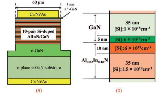
VCSELs generally use structures called distributed Bragg reflectors to provide the necessary reflectivity for an effective cavity that allows the device to lase. These reflectors are alternating layers of materials with different refractive indices, which result in a very high reflectivity. Intracavity contacts can help improve the poor conductivity of GaN VCSELs, but these increase the cavity size leading to poor optical confinement, complex fabrication processes, high threshold current densities and a low output-versus-input power efficiency (i.e. the slope efficiency).
The low conductivity in DBR structures is the result of polarization charges between the layers of different materials – AlInN and GaN. To overcome the effects of polarization charges, Takeuchi and colleagues used silicon-doped nitrides and introduced “modulation doping” into the layers of the structure. The increased silicon dopant concentrations at the interfaces help to neutralize the polarization effects.
Meijo and Nagoya University researchers have also devised a method to expedite the AlInN growth rate to over 0.5 μm/h. The result is a 1.5λ-cavity GaN-based VCSEL with an n-type conducting AlInN/GaN distributed Bragg reflector that has a peak reflectivity of over 99.9% , threshold current of 2.6 mA, corresponding to a threshold current density of 5.2 kA/cm2, and an operating voltage was 4.7V.
Reference and Affiliation
Kazuki Ikeyama1, Yugo Kozuka1, Kenjo Matsui1, Shotaro Yoshida1, Takanobu Akagi1, Yasuto Akatsuka1,
Norikatsu Koide1, Tetsuya Takeuchi1*, Satoshi Kamiyama1, Motoaki Iwaya1, and Isamu Akasaki1,2. Room-temperature continuous-wave operation of GaN-based vertical-cavity surface-emitting lasers with n-type conducting AlInN/GaN distributed Bragg reflectors. Applied Physics Express 9, 102101 (2016)
http://doi.org/10.7567/APEX.9.102101
- Faculty of Science and Technology, Meijo University, Nagoya 468-8502, Japan
- Graduate School of Engineering and Akasaki Research Center, Nagoya University, Nagoya 464-8603, Japan