22 September 2016
Plasmons are key players when trying to squeeze light into tiny circuits and control its flow electrically. Last year, the nano-optoelectronics research group led by ICREA Prof. at ICFO Frank Koppens, showed that high-quality graphene could guide plasmons and confine them to length scales of nanometers, one hundred to two hundred times below the wavelength of light, yet while maintaining a long plasmon lifetime. However, one missing link in this picture was the lack of an on-chip detector of plasmons.
Now, their investigation has gone a huge step forward. In a recent study, published in Nature Materials, ICFO researchers Dr. Mark Lundeberg and Achim Woessner, led by ICREA Prof. at ICFO Frank Koppens, in collaboration with CIC nanoGUNE, Columbia University and the National Institute for Materials Science in Japan, have been able to fabricate an all-graphene mid-infrared plasmon detector operating at room temperature, where a single graphene sheet serves simultaneously as the plasmonic generation medium and detector.
In their study, the team of scientists used a new experimental design in which they employed two local gates—a split metal sheet located underneath the graphene—to fully tune the thermoelectric and plasmonic behaviour of the graphene. In contrast to the conventional back gating through a thick SiO2 layer, the separate local gates not only induce free carriers in the graphene to act as a plasmonic channel, but also create a thermoelectric detector for the plasmons. The resulting device converts the conveniently available natural decay product of the plasmon, electronic heat, directly into a voltage through the thermoelectric effect.
The results of this paper open a new pathway to graphene ´plasmo-electronics´, which would allow to perform mid-infrared opto-electronics at very small length scales. The team looks forward to creating a fully integrated system in which all three parts, source, channel, and receiver, are made of graphene, enabling a new ´all-carbon optics´ technology.
Graphene does double duty for plasmons
An ICFO study published in Nature Materials demonstrates how graphene can be employed simultaneously as both a plasmonic medium and detector
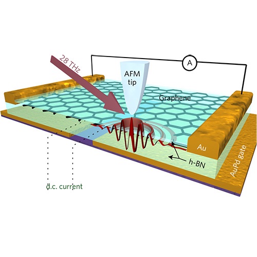
Schematic cross-section of device and measurement technique. [credit: Achim Woessner/ICFO]


