April 20, 2016
Bri Buckley
Nathan Gray, Ph.D.
Tom Darnall
Infrared (IR) imaging systems rely on a key cost-driving component, the focal plane array (FPA). Many IR FPAs use Indium Antimonide (InSb) wafers, and resulting image-device performance depends on the electronic and crystallographic properties of the wafer.
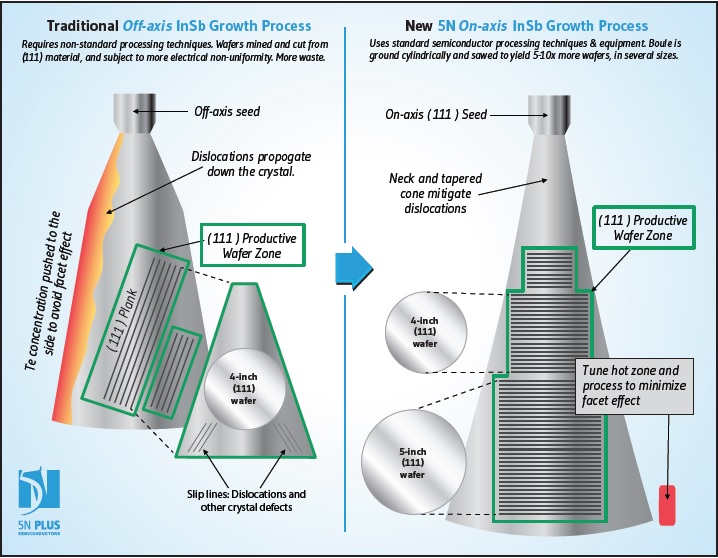
Focal plane arrays are fabricated on the polished surface of a (111) oriented wafer. For the last 60 years, industry standard InSb wafers have been derived from a crystal grown several degrees off-axis from the <111> orientation. Unfortunately, this approach results in relatively low yields because the electrical properties of the wafers can vary significantly. FPA devices made from these wafers can exhibit inconsistent device response and performance.
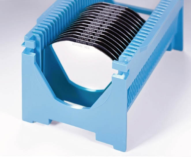
5N Plus Semiconductors has developed a process for growing large-diameter InSb crystals on the <111> axis. For the first time, a single crystal can yield hundreds of wafers, with far less material waste, and using established high-volume manufacturing methods. This is a five- to ten-fold improvement over traditional methods. The resulting InSb wafers, 50 to 150 mm in diameter, are consistent in their electrical properties, which translates to higher FPA yields for manufacturers and lower engineering costs.
How the facet effect has discouraged innovation
One challenge in producing consistent and reliable InSb wafer products is controlling the “facet effect,” which describes the effect of anisotropic dopant segregation that occurs during crystal growth, resulting in non-uniform properties.

When the segregation coefficient of the dopant changes significantly across the melt/solid interface of a growing crystal, it causes inconsistent electrical properties in wafers made from those crystals. This issue is more pronounced in InSb crystal growth than in other semiconductor materials and compounds, and is more likely to occur when crystals are grown on-axis. For this reason, InSb wafer manufacturers have historically avoided the facet effect by growing off-axis and accepting lower yields.
Because off-axis growth also limits crystal size, the diameter and quantity of wafers produced from these crystals are also limited. Standard semiconductor manufacturing techniques cannot be used, because the off-axis crystal must first be cropped to a <111> orientation to produce wafers for FPAs. This reduces process reliability and leads to relatively low wafer yields, as well as inconsistent electrical properties in the wafers.
Determined to overcome these wafer-manufacturing limitations, 5N Plus scientists spent several years developing a new crystal-growth process. The project demanded new techniques for controlling the facet effect during crystal growth, explained later in this paper. Industry experts were skeptical, because others had tried this approach and failed. But the 5N Plus team persevered, and their efforts resulted in large diameter, low-dislocation InSb crystals that each yield hundreds of high-performance wafers with uniform electrical properties.
A brief history of InSb crystal-growth technology
The material properties of InSb make it highly desirable for military and commercial applications in the mid-wave infrared (MWIR) range. It’s a popular choice for “cooled” focal-plane arrays that typically operate at liquidnitrogen temperature (77 K, or −320 °F). InSb has a very narrow bandgap of 0.17 eV at 300 K, the lowest bandgap binary compound in the III-V semiconductor family, and is well-suited for MWIR sensors.
InSb crystal-growth technology has been evolving for more than 60 years. A variety of methods were tested during the 1950s and 1960s, including zone melting, and both horizontal and vertical Bridgman. These methods produced smalldiameter crystals with a high density of crystal defects.
Czochralski crystal growth was first attempted in 1965 by S.G. Parker, who found that the method produced InSb crystals of higher quality and larger diameter. This soon became (and still is) the industry-standard method of growing InSb crystals. Russian scientists made some progress controlling the facet effect, but they were only successful on a research scale; the resulting crystals were very small (~ 2 inches).
The Czochralski method alone does not eliminate crystal defects. Producing InSb crystals with low dislocation density is considerably more challenging than growing single-element crystals of silicon and germanium. The energy barrier to form defects during the growth process is lower, and the difference in segregation coefficients is much larger. When doped with tellurium, the facet effect contributes to non-uniform distribution of the dopant across this reason, most manufacturers avoid the facet effect and grow crystals off-axis instead, accepting the production trade-offs described above.
Manufacturers of IR FPAs require polished (111) InSb wafers. When InSb crystals are grown off-axis, the process is limited, and does not permit techniques that can minimize dislocation formation. As a result, traditional wafer manufacturing relies on cropping and recovering as much <111> oriented material as can be “mined” from the crystal. This method avoids defects and regions of non-uniform dopant distribution, but can result in less acceptable material and higher production costs.
How 5N Plus is transforming the process
The team at 5N Plus was highly motivated to tackle the challenges of on-axis crystal growth and develop a more controlled process. Like other manufacturers, the company began growing InSb crystals off-axis and then mining for wafers, but when it moved its InSb operations to a new location, the team began exploring the use of proven semiconductor manufacturing practices.
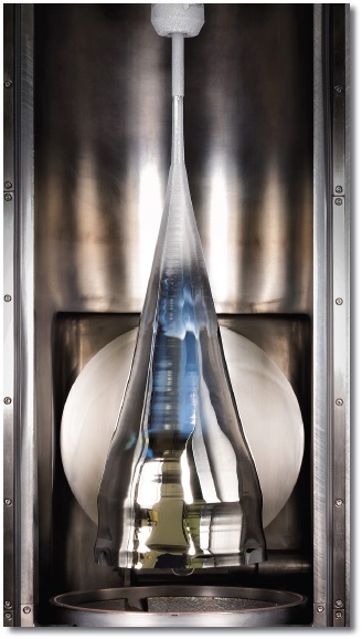
InSb crystal still attached in puller housing
5N Plus is the first to develop and refine an industry standard process for growing large-diameter InSb crystals “on axis” (), promising higher process yields and lower engineering costs for FPA manufacturers.
In IR FPA fabrication, signal-to-noise ratio and detector photo response are vital. InSb crystal dislocations can disrupt charge transport through the affected part of a wafer and decrease electrical performance. This leads to higher resistance, lower signal-to-noise ratios and non-uniform detector response in the IR sensor. Such defects manifest in FPAs as dead or dark pixels and pixel clusters and uneven photo-response, and little can be done in FPA production to correct these issues.
5N’s biggest challenge was controlling the facet effect, which required controlling dopant incorporation over the melt/solid growth interface. Scientists had to exert precision control over the melt stoichiometry, the melt/solid interface, and all of the ambient conditions that affect crystal growth.
X-ray topography analysis was used to determine the process parameters that result in the fewest defects. The team knew dislocations and other structural defects are often the result of stress at the growth surface, which is linked to unstable temperatures and material impurities or foreign particles.
In addition, the Dash Necking Method was used to reduce stress at the growth interface. Process engineers reduce thermal shock imparted to the crystal when it detaches from the melt by controlling the shape of the crystal’s tail.
Ultimately, 5N’s team figured out how to grow large InSb crystals on-axis by redesigning the hot zones in the puller and by precisely controlling growth parameters such as the pull rate. The resulting InSb boules have few dislocations and allow large wafers to be produced efficiently with uniform electrical properties.
Growing on-axis also means 5N’s crystal structures are more symmetrical, allowing for lower-stress growth conditions. Larger diameter crystals are easier to make because the superior structure can handle additional weight without breaking at the neck. In addition, the team now applies standard crystal defect-reduction techniques that were not possible with off-axis growth.
An industry-standard crystal growth process results in fewer defects and dislocations in the crystal structure, eliminating the need to mine for good material. Low-defect crystals also enable high-volume manufacturing techniques and do away with inconsistencies inherent in old-fashioned wafer processing methods. For example, 5N’s crystals can be sawed with a multiple-wire saw, producing up to 100 wafers in a single cut.
5N’s approach mean higher FPA yields and lower engineering costs
Even after experts said, “It couldn’t be done,” 5N Plus now successfully grows InSb crystals and fabricates high-performance wafer substrates in a way no other company does.
The company’s on-axis crystal-growth method results in high-quality InSb wafer products in a variety of diameters and with uniform electrical performance. Because the process minimizes dislocations and other structural defects, these wafers provide downstream benefits for FPA device manufacturing, including higher device yields and lower engineering costs.
5N InSb crystals look different from InSb crystals grown by traditional manufacturers. That’s because they are different. And better.
For more information about on-axis InSb crystal growth and InSb wafers,
contact Paul McKay at (250) 231-0280 or paul.mckay@5nplus.com,
or Dr. Nathan Gray at (435) 669-2939 or nathan.gray@5nplus.com.


