(17-02-2015) Scientists from Ghent University and imec have announced that they demonstrated interaction between light and sound in a nanoscale area.
Their findings elucidate the physics of light-matter coupling at these scales – and pave the way for enhanced signal processing on mass-producible silicon photonic chips.
In the last decade, the field of silicon photonics has gained increasing attention as a key driver of lab-on-a-chip biosensors and of faster-than-electronics communication between computer chips. The technology builds on tiny structures known as silicon photonic wires, which are roughly a hundred times narrower than a typical human hair. These nanowires carry optical signals from one point to another at the speed of light. They are fabricated with the same technological toolset as electronic circuitry.
Fundamentally, the wires work only because light moves slower in the silicon core than in the surrounding air and glass. Thus, the light is trapped inside the wire by the phenomenon of total internal reflection. Simply confining light is one thing, but manipulating it is another. The issue is that one light beam cannot easily change the properties of another. This is where light-matter interaction comes into the picture: it allows some photons to control other photons.
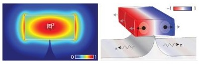
Publishing in Nature Photonics, researchers from the Photonics Research Group of Ghent University and imec report on a peculiar type of light-matter interaction. They managed to confine not only light but also sound to the silicon nanowires. The sound oscillates ten billion times per second: far more rapid than human ears can hear. They realized that the sound cannot be trapped in the wire by total internal reflection. Unlike light, sound moves faster in the silicon core than in the surrounding air and glass. Thus, the scientists sculpted the environment of the core to make sure any vibrational wave trying to escape it would actually bounce back. Doing so, they confined both light and sound to the same nanoscale waveguide core – a world’s first observation.
Trapped in that incredibly small area, the light and vibrations strongly influence each other: light generates sound and sound shifts the color of light, a process known as stimulated Brillouin scattering. The scientists exploited this interaction to amplify specific colors of light. They anticipate this demonstration to open up new ways to manipulate optical information. For instance, light pulses could be converted into sonic pulses and back into light – thereby implementing much-needed delay lines. Further, the researchers expect that similar techniques can be applied to even smaller entities such as viruses and DNA. These particles have unique acoustic vibrations that may be used to probe their global structure.
R. Van Laer, B. Kuyken, D. Van Thourhout and R. Baets. Interaction between light and highly confined hypersound in a silicon photonic nanowire. Nature Photonics (2015) http://dx.doi.org/10.1038/nphoton.2015.11
The Photonics Research Group in the Department of Information Technology of Ghent University is active in the field of photonic integration - more specifically silicon photonics - and its applications in information and communication technology, in sensing and in life sciences.
The group puts its research focus on new concepts for photonic integrated devices and circuits and on the associated technologies and design methodologies. This includes passive and active waveguide-based photonic components, based on CMOS-compatible materials and processes as well as hybrid approaches combining silicon with other functional materials. The activities center around the telecom wavelength of 1.55 micrometer but are expanding both to longer wavelengths (mid-IR) and shorter wavelengths (visible). The infrastructure of the group includes cleanroom facilities for in-house fabrication of components as well as a variety of CAD-tools and measurement labs. The group is associated with the nano-electronics research center imec in Leuven and uses the CMOS-oriented research facilities of imec for research on silicon photonics.


