February 4 , 2015
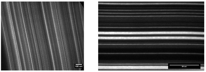
Researchers at aBeam Technologies, Lawrence Berkeley National Laboratory and Argonne National Laboratory have developed a technology to fabricate test patterns with a minimum linewidth down to 1.5 nm. The fabricated nanostructures are used to test metrological equipment. The designed patterns involve thousands of lines with precisely designed linewidths; these lines are combined in such a way that the distribution of linewidths appears to be random at any location. This pseudo-random test pattern allows nanometrological systems to be characterized over their entire dynamic range.
The test pattern contains alternating lines of silicon and tungsten silicide, this results in a pretty good contrast in the metrological systems. The size of the sample is fairly large, apprx. 6x6 microns, and involves thousands of lines, each according to its designed width. Earlier, aBeam and LBNL reported the capability of fabricating 4 nm lines and spaces using e-beam lithography, atomic layer deposition, and nanoimprint, see http://nanotechweb.org/cws/article/lab/48111.
Dr. Sergey Babin, president of aBeam Technologies said: “The semiconductor industry is moving toward a half-pitch of 11 nm and 7 nm. Therefore, metrology equipment should be very accurate, at least one order of magnitude more accurate than that. The characterization of metrology systems requires test patterns at a scale one order smaller than the measured features. The fabrication was a challenge, especially for such a complex pattern as a pseudo-random design, but we succeeded.”
Dr. Valeriy Yashchuk, a researcher at the Advanced Light Source of LBNL continued: “When you measure anything, you have to be sure that your metrological system produces accurate results, otherwise what kind of results will you get, nobody knows. Qualifying and tuning metrology systems at the nanoscale is not easy. We designed the test pattern that is capable of characterizing nano-metrology systems over their entire dynamic range, resulting in the modulation transfer function, the most comprehensive characteristic of any system.”
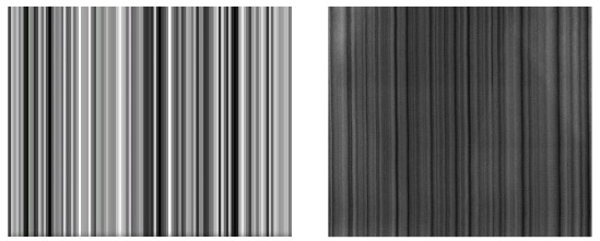
(a) A part of the designed pseudo-random test sample and (b) SEM image of the test sample.
The test pattern is to be used to characterize almost any nano-metrology system. Experiments were performed using a scanning electron microscope (SEM), atomic force microscope (AFM), and soft x-ray microscopes. A part of an ideal test-sample and its SEM microscopy image is shown below. The image includes imperfection in the microscope and needs to be characterized.
The power spectral density of the sample is flat; the spectra of the image has a significant cut-off at high frequencies; this is used to characterize the microscope over its dynamic range and show the degradation of the microscope’s sensitivity as soon as the linewidth becomes smaller.
About the authors
This project was led by Dr. Sergey Babin, president of aBeam Technologies, Dr. Valeriy Yashchuk of Lawrence Berkeley National Laboratory and Dr. Ray Conley of Argonne National Laboratory and Brookhaven National Laboratory. This work was supported by the Department of Energy under the contract #DE-SC0011352 in the framework of a STTR project. Work at LBNL, ANL, and BNL was supported by the Department of Energy, Office of Basic Energy Sciences under contracts no. DE-AC02-05CH11231, DE-AC0206CH11357, and DE-SC00112704 respectively, and by Grant ID No. 268826.


