December 02, 2014
In quantum optics, generating entangled and spatially separated photon pairs (e.g. for quantum cryptography) is already a reality. So far, it has, however, not been possible to demonstrate an analogous generation and spatial separation of entangled electron pairs in solids. Physicists from Leibniz University Hannover and from the Physikalisch-Technische Bundesanstalt (PTB) have now taken a decisive step in this direction. They have demonstrated for the first time the on-demand emission of electron pairs from a semiconductor quantum dot and verified their subsequent splitting into two separate conductors. Their results have been published in the current online issue of the renowned journal "Nature Nanotechnology".
A precise control and manipulation of quantum-mechanical states could pave the way for promising applications such as quantum computers and quantum cryptography. In quantum optics, such experiments have already been performed for some time. This, for example, allows the controlled generation of pairs of entangled, but spatially separated photons, which are of essential importance for quantum cryptography. An analogous generation and spatial separation of entangled electrons in solids would be of fundamental importance for future applications, but could not be demonstrated yet. The results from Hannover and Braunschweig are a decisive step in this direction.
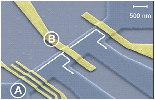
As an electron source, the physicists from Leibniz University Hannover and from PTB used so-called semiconductor single-electron pumps. Controlled by voltage pulses, these devices emit a defined number of electrons. The single-electron pump was operated in such a way that it released exactly one electron pair per pulse into a semiconducting channel. A semitransparent electronic barrier divides the channel into two electrically distinct areas. A correlation measurement then recorded whether the electron pairs traversed the barrier, or whether they were reflected or split by the barrier. It could be shown that for suitable parameters, more than 90 % of the electron pairs were split and spatially separated by the barrier. This is an important step towards the envisioned generation and separation of entangled electron pairs in semiconductor components.
The original publication:
Niels Ubbelohde, Frank Hohls, Vyacheslavs Kashcheyevs, Timo Wagner, Lukas Fricke, Bernd Kästner, Klaus Pierz, Hans W. Schumacher, Rolf J. Haug: Partitioning of on-demand electron pairs. Nature Nanotechnology (2014), doi: 10.1038/nnano.2014.275
http://www.nature.com/nnano/journal/vaop/ncurrent/full/nnano.2014.275.html


