Ditzingen, April 18, 2013 – The pace of technical development in the computer and electronics industries has been more than swift. Who, twenty years ago, would have dreamed of the functions today’s mobile phone or tablet PC can execute – to say nothing about setting up a continuous link to the Internet. This has been made possible by ever smaller and ever more powerful microchips. As early as 1965, Intel co-founder Gordon Moore postulated “Moore’s Law”, an axiom that would have far-reaching effects on the semiconductor industry and its technology roadmaps. This law says that the number of transistors on any given surface area will double every 18 months, accompanied by a simultaneous decline in costs. Since then, the semiconductor industry has waged a billiondollar battle for each square nanometer.
Microlithography is used to produce these integrated circuits. A lithography system projects the miniaturized image of a circuit onto a silicon wafer, exposing a layer of photoresist applied in advance. Abbe’s theory of imaging says that a light source cannot reproduce any structures smaller than its own wavelength. This resolution limit has in the meantime proven to be flexible. At present, lithography systems working with a wavelength of 193 nanometers are creating structures only 22 nanometers in size. Several tricks are used to achieve this. One example is double patterning – carrying out each exposure step twice. Immersion is also used. In this variation, the greater refractive index of water is used during exposure in order to achieve even shorter wavelengths. The light sources now in use, however, are slowly reaching the limits of both resolution and economy. In an attempt to comply with Moore’s Law through 2030 and beyond, the leading companies in the semiconductor industry launched the extreme ultraviolet (EUV) lithography project more than a decade and a half ago. The goal was to develop a generator for EUV light with its wavelength of 13.5 nanometers. This technology makes it possible to image structural elements less than ten nanometers in size. This corresponds to more than ten billion transistors on a microchip.
The greatest challenge in EUV lithography is generating light with a wavelength of 13.5 nanometers. A number of different strategies are striving for market acceptance and the most successful to date is generation using a so-called laser produced plasma, or LPP in short. Tin drips into a vacuum chamber; a flash of laser light strikes and ionizes a falling droplet. This gives rise to a plasma flash of the desired wavelength. The EUV light is captured in a collector, bundled, and passed along to the lithography system to expose the wafer.
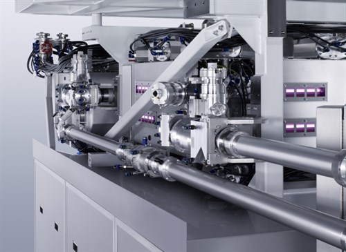
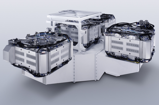
Amplification
Power gain in a TRUMPF Laser Amplifier. To boost the output pulse, the laser active medium is amplified in several tubes.
Photo: TRUMPF Group
Achieving a profitable manufacturing process requires 50,000 hits per second. The TRUMPF Laser Amplifier provides the CO2 pulse needed for this purpose. Based on a continuouswave CO2 laser in the ten-kilowatt output range, TRUMPF has developed a pulsed CO2 laser system. The five amplifier stages in this system boost a CO2 laser pulse, with its mean power of a few watts, by a factor in excess of 10,000 to more than 20 kilowatts of mean pulse power – while peak pulse power comes to several megawatts. TRUMPF provides the components for this complex system. When making its contribution to this project, the company draws on its vast experience with CO2 lasers, stretching back almost thirty years. Since the spring of 2012, TRUMPF has supplied several second-generation laser systems to firms that manufacture the lithography systems. EUV lithography is now making its appearance on the production lines where ICs are manufactured. Using these concepts, developers are already imaging structural elements measuring only 13.8 nanometers – half the size of a virus. The single-digit nano range – as large as the diameter of a DNA strand – is now within reach. Industrial users have long valued the TRUMPF CO2 laser as a robust beam for heavy work. Now it is opening the gates to the future of semiconductor production.